Analysis of electronic parts
Boosting Productivity
ZEISS improves workflows, data flow and decision-making during electronic part analysis.
ZEISS offers a unique portfolio of optical 3D scanners, CT systems, industrial microscopes and sensors for the dynamic capture of 3D deformations. Data correlation – even if the data comes from different sources – accelerates the workflow of analyses and decision-making processes.
Manufacturers of classic consumer electronics, such as computers or smart home solutions, are by no means the only producers who need electronic chips for their products. The demand for high-performance electronics and sensors is also soaring in the automotive industry, medical technology and trade logistics. The food industry already uses microchips for smart packaging.
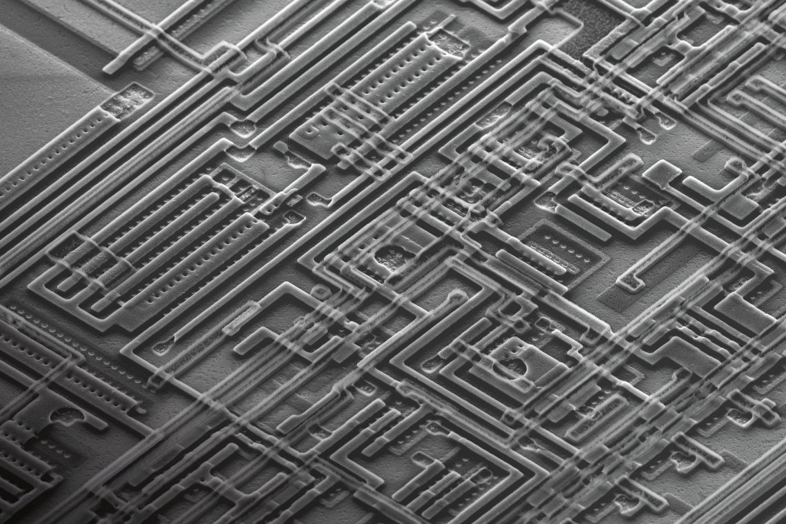
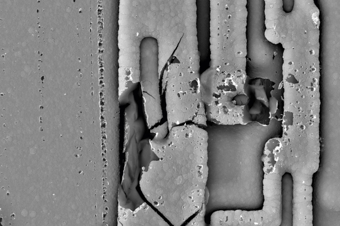
Defects and impurities in the micrometer range: ZEISS solutions assist users during defect localization, root cause analysis and decision-making processes.
In the automotive industry, electronic parts must meet especially stringent requirements: Today, more than 100 control units already include computer programs which are managing a multitude of vehicle functions. Going forward, trends like autonomous driving will lead to even more complex control electronics. Connectivity requirements, especially for e-cars, are also evolving very rapidly. Quality assurance is facing new and consistently hard challenges, because the design of individual parts is complex and expensive. But there is even more to it than that: The parts must be resistant to loads over a long period of time, such as temperature fluctuations or vibrations. Even the smallest defect can have a massive impact. It is therefore all the more important to analyze those defects – for quality assurance, but also to keep productivity high.
ZEISS offers a broad portfolio for seamless quality assurance that covers all applications from research and development to quality control on the shop floor and outbound inspections: In addition to defect analysis and metallography, this also includes load tests and the analysis of part quality.
Intuitive workflow for technical cleanliness
Contamination with very fine particles are a growing problem when dealing with complex systems. Critical particles can cause a malfunction, for example, a short circuit on a printed circuit board. Number, size, chemical composition and origin of these particles are determined in a two-stage process using a light and electron microscope. The results are then displayed in a tabular categorized form in the ZEISS Technical Cleanliness Analysis software.
Real-time measurements in research and development
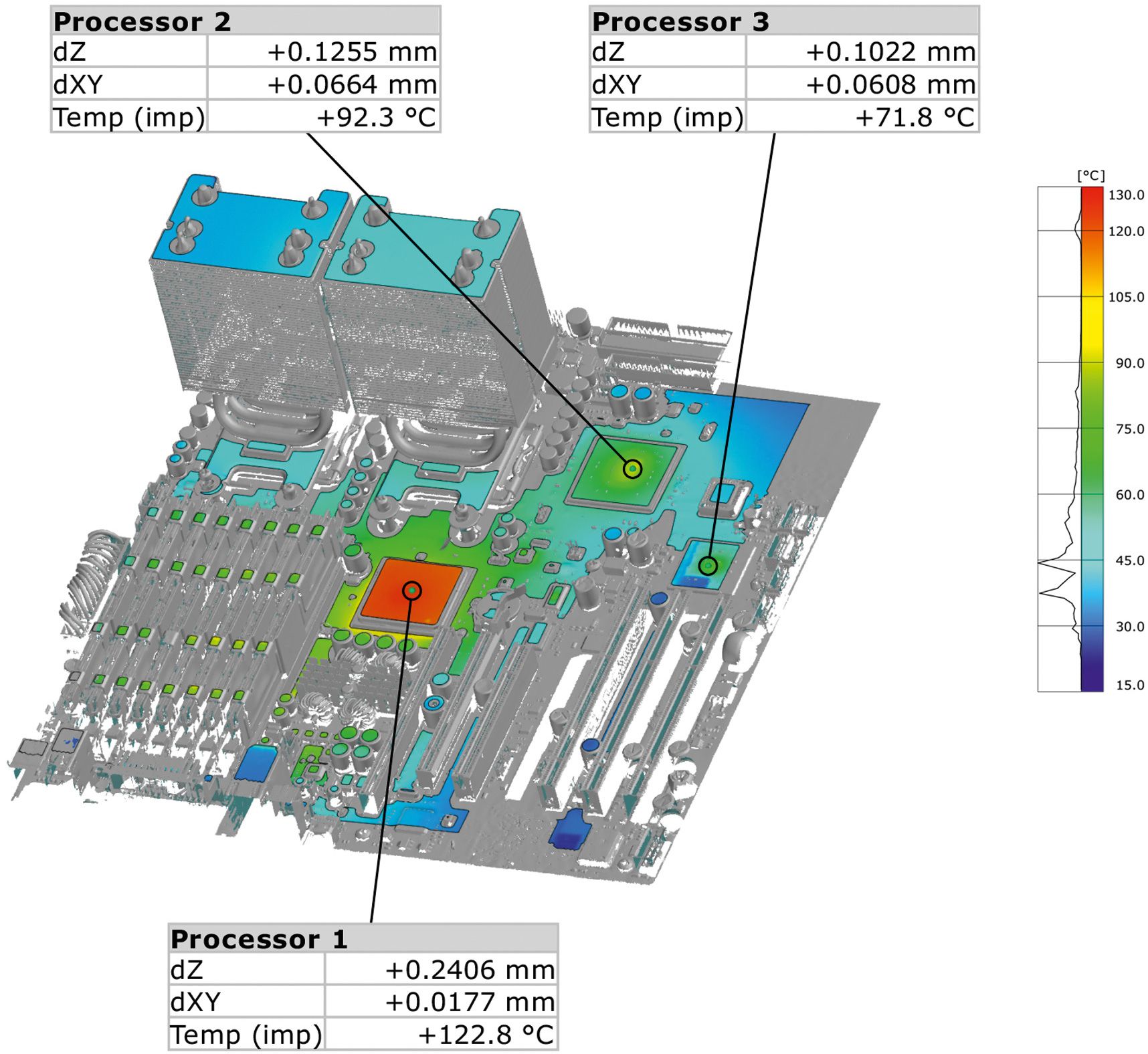
3D analyses help to optimize parts in research and development. Users can analyze the behavior of electronic parts under thermal and mechanical loads in real time in order to identify critical areas and deformations on circuit boards. ARAMIS carries out non-contact 3D motion and deformation analyses down to the submicrometer range.
Benefits of combined data analysis
The analysis workflow is based on certain objectives: As soon as a part shows irregularities in the functional test, a computed tomography is done as a first step to identify critical areas. The exact defect position is then forwarded via a software inferface to a microscope which conducts a deeper analysis of the malfunction.
Deformations of the part are measured dynamically and are included in the analysis workflow.

“This means users will have more time to focus on interpreting the results and taking decisions.”