Scanning electron microscopes and AI tools
Close Investigation
Optimizing manufacturing with scanning electron microscopes and AI tools
The demands on quality and performance constantly increase – and with them the need to obtain even more detailed information about parts and their materials. When analytical methods of light microscopy reach their limits, more and more companies therefore turn to high-resolution scanning electron microscopes.
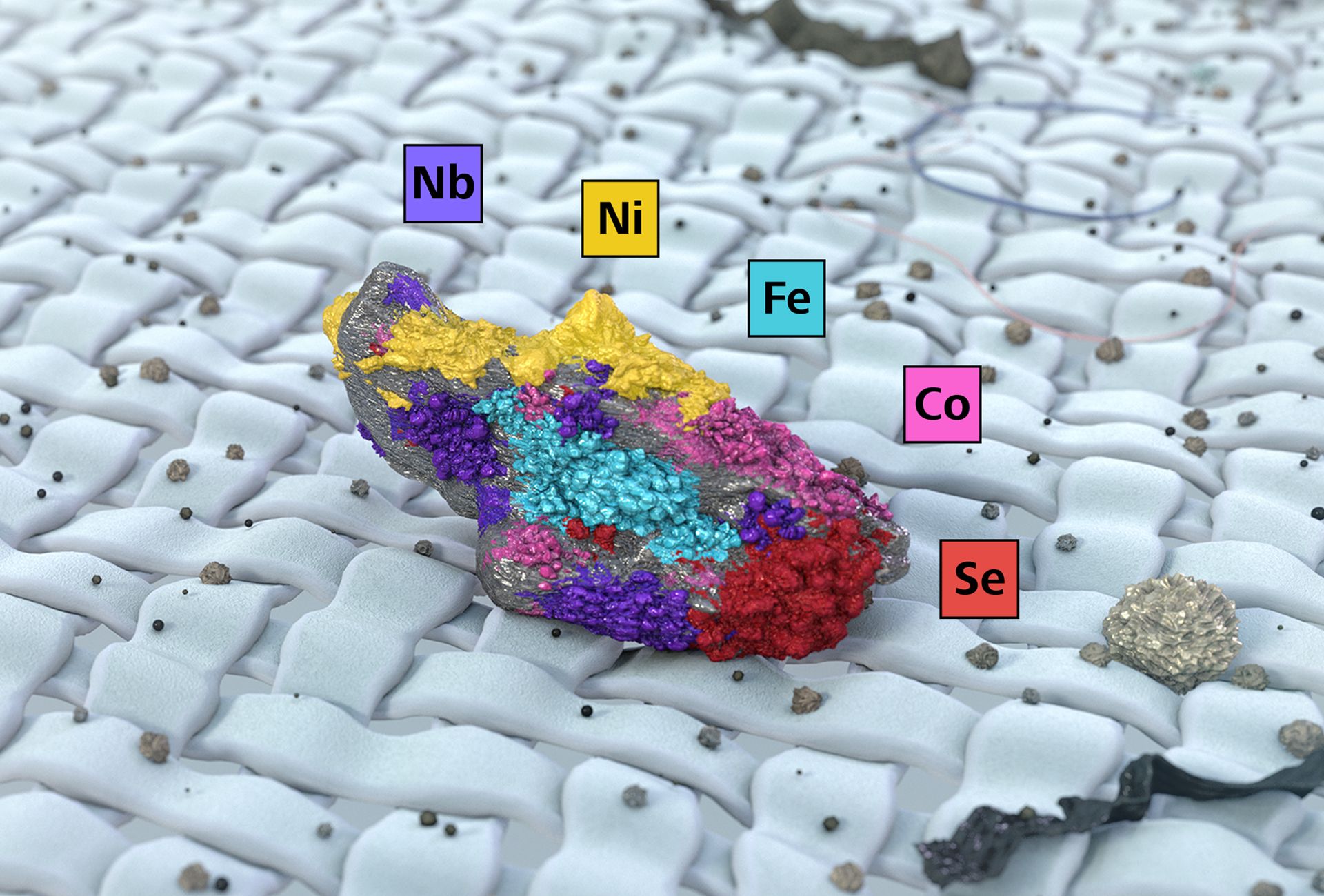
With a scanning electron microscope, an object is scanned with a finely bundled electron beam, which delivers a significantly higher resolution than light microscopes. Using X-ray spectroscopy (EDX), it can even be used to determine the chemical composition of elements. While the systems are standard in research, companies are starting to catch up by utilizing scanning electron microscopes in quality control for different tasks, such as failure analysis on batteries, inspection of metal alloys, plastics, steel and composite materials or investigation and characterization of new materials. ZEISS offers a broad portfolio of systems that can be used for various quality-assurance applications.

Highest resolution & elemental analysis:
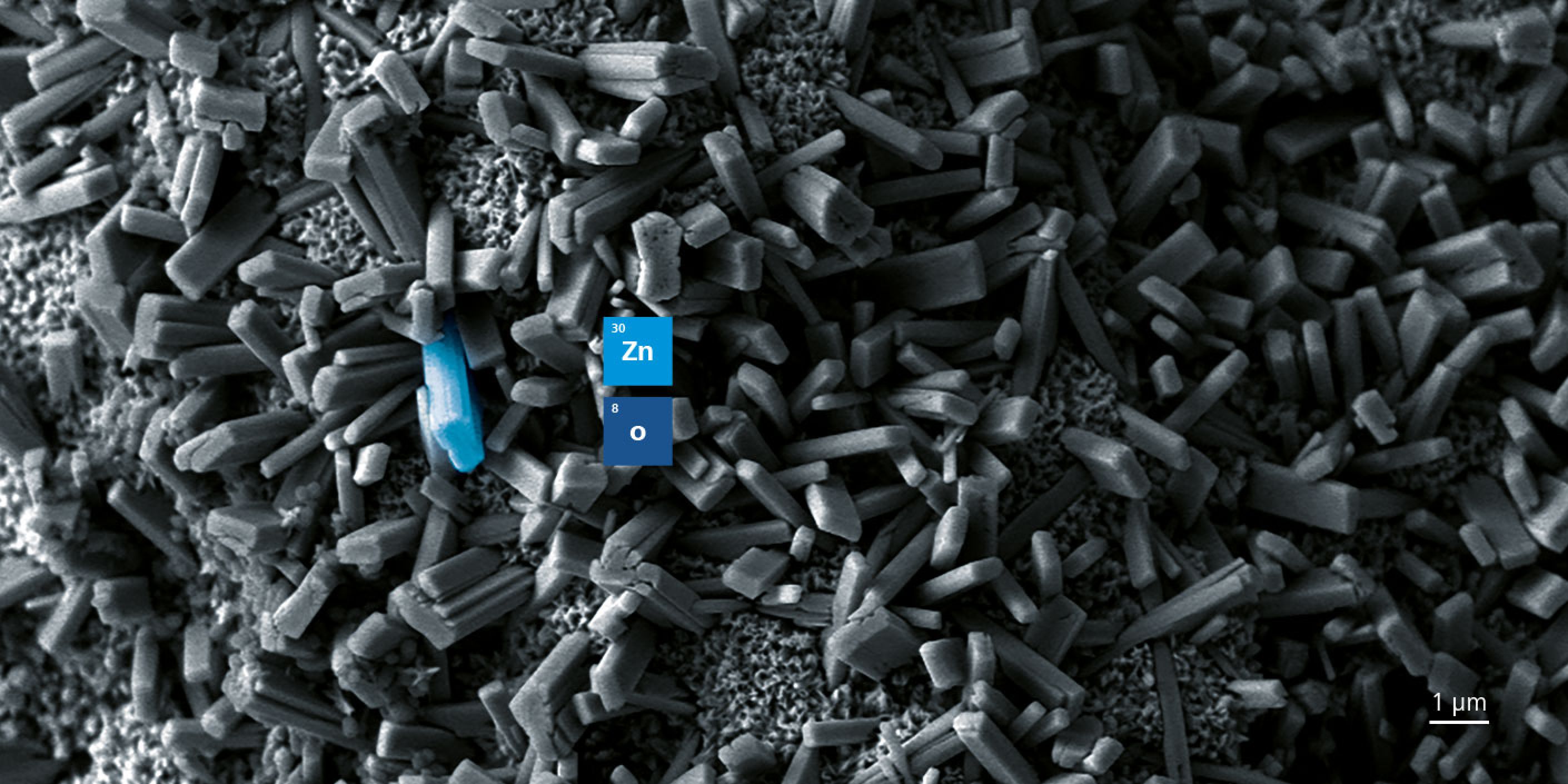
This image of zinc oxide dendrites aids detection of morphological changes in the electrodes of energy storage systems. It was captured with the field emission scanning electron microscope ZEISS Sigma.
The ZEISS EVO product family offers high-performance models for the start into the world of high resolution imaging. High performance, intuitive operation and future-proof upgradability options are the hallmarks of the family.
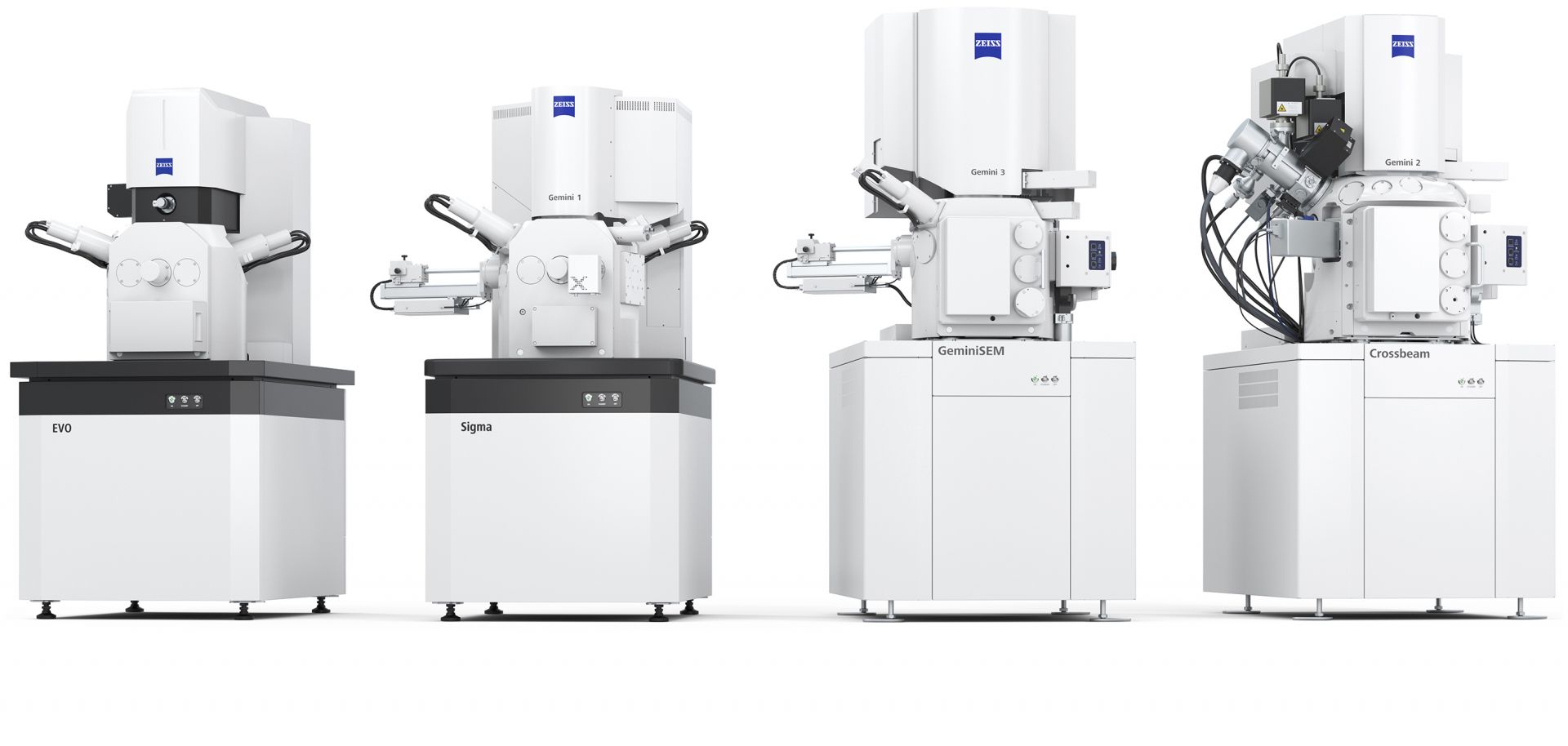
The ZEISS SIGMA product family allows for a more extensive analysis depicting surfaces and nanostructures. Especially microelectronic components, medical implants and samples from polymer materials can be investigated in a precise, reproducible way.
The ZEISS GeminiSEM product family delivers an outstanding depth of field with razor-sharp, subnanometer resolutions. The systems are used for the high-precision structural analysis of components or super-thin layers. Brand-new features help perform uncompromisingly high-quality EDX analysis on non-conductive material.
The ZEISS Crossbeam product family provides insight into the interior of a sample by local material ablation by a focused ion beam and an integrated femtosecond laser. This exposes high-contrast cross sections for SEM imaging in the third dimension. Likewise, the system stands for automated TEM lamella preparation workflows.
Integrated solutions for industrial microscopy
Apart from the hardware, ZEISS provides both integrated solutions such as correlative microscopy as well as image analysis through deep learning, which provides noticeable improvements as to information, workflow and the presentation of results.
Technical cleanliness
AI as efficiency booster: ZEISS software speeds up the classification of particles
Modern manufacturing processes and quality requirements intensify the demands on technical cleanliness from the raw material to the finished product. To increase resource efficiency and optimize the time-consuming classification of process-critical particles, ZEISS offers the Technical Cleanliness Analysis module. The software module has been pre-trained with correctly classified particles and combines classical analysis with AI-based object classification models. With faster and more selective results, the module ensures a better utilization of both the microscope and the operators, who are no longer tied up by the otherwise necessary rework.